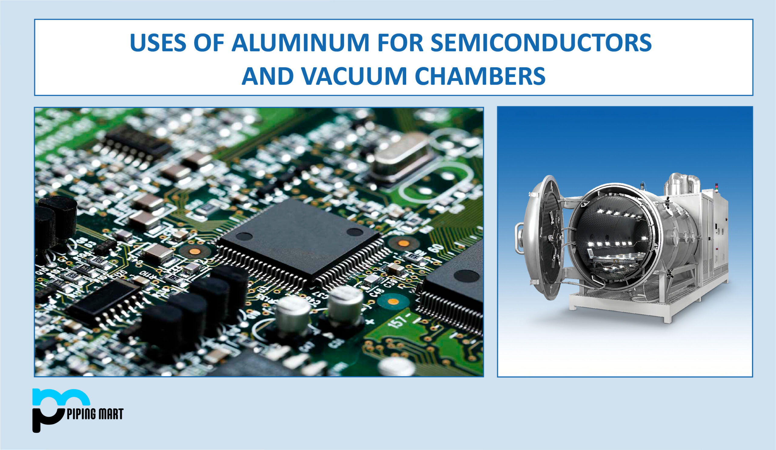
Aluminum Applications For Vacuum Chambers And Semiconductors
Vacuum chambers and semiconductors are one area in the aluminum business that doesn’t get enough attention. These highly technical industries have strict material requirements; only specified grades are acceptable. With its many advantages and outstanding performance, aluminum is the ideal material for such demanding applications.
Although these two technologies are very different, there is some crossover because semiconductors must be manufactured and tested in vacuum or inert gas environments. Aluminum is used to satisfy several of the material requirements that are specific to each application.
What are vacuum chambers?
All air and other gases are drawn from an enclosed space to create a vacuum chamber using a vacuum pump. The chamber’s low-pressure atmosphere makes it possible to perform scientific research and test equipment that could need to function in vacuum-like circumstances (including outer space). When gases are added to a vacuum chamber after ambient air has been removed, a gaseous environment is created that is necessary for further procedures. Other mechanical processes, such as vacuum drying and coating, call for this equipment.
These enclosures are typically made of ceramic, glass, and acrylic or metals like aluminum, stainless steel, and brass. These materials offer varying degrees of protection from outside magnetic fields based on their thickness, resistivity, and permeability. Aluminum has a high strength-to-weight ratio and other advantages that make it a preferred choice for vacuum chambers.
Multiple ports with vacuum flanges must be included when building a vacuum chamber so that instruments can enter. The sealing of these ports will rely on the technical requirements. Elastomer o-rings may be employed in low-vacuum settings. Knife edges will be machined into the flanges in high-vacuum situations, and as the flange is bolted on, they will be cut into a metal gasket.
Why is aluminum a good choice for vacuum chambers?
Due to its various advantages, aluminum is an excellent choice for vacuum chambers. First off all, because of its immense strength, it can survive the enormous pressure and stresses that a vacuum chamber will subject it to. It is best used in situations where exposure to chemicals or the environment could reduce an application’s longevity due to its better corrosion resistance.
Additionally, there are unique conditions that only apply to vacuum chambers. Compared to stainless steel, aluminum exhibits hydrogen permeability that is seven orders of magnitude lower. This indicates a lower likelihood of hydrogen gas, water, or hydrocarbon vapor contamination in an aluminum vacuum chamber. Compared to other metals like stainless steel, aluminum allows less carbon contamination. This increases protection from vacuum contamination by carbon gas, much like hydrogen.
The thin layer of aluminum oxide that forms naturally on aluminum serves as a barrier to lessen the transfer of pollutants like hydrogen, oxygen, and carbon, which is another advantage of dealing with aluminum alloys. Other benefits include the simplicity of anodization, excellent vibration dampening, reduced residual radiation, and other advantages we haven’t yet discussed, such as improved machinability and formability, which make working with aluminum simple.
What is a semiconductor?
An electronic component known as a semiconductor device uses electrical conduction and possesses properties that fall in between those of a conductor, like copper, and an insulator, like glass. These gadgets have replaced vacuum tubes in most contemporary applications because they use solid-state electrical conduction rather than gaseous conduction or thermionic emission in a vacuum.
Integrated circuit chips are where semiconductors are most frequently used. A single semiconductor wafer may house billions of small semiconductors integrated into single chips interconnected in our contemporary computing gadgets, including mobile phones and tablets.
A semiconductor’s conductivity can be changed in several ways, including applying an electric or magnetic field, exposing it to light or heat, or deforming a grid of doped monocrystalline silicon. Although the technical justification is extensive, manipulating semiconductors made our contemporary digital revolution possible.
How is aluminum used in semiconductors?
Due to its various advantages, aluminum is frequently used in semiconductors and microchips. For instance, silicon dioxide, a key component of semiconductors, adheres to aluminum more effectively than silicon dioxide (this is where Silicon Valley got its name). Another advantage of aluminum is that it has low electrical resistance and provides excellent contact with wire bonds due to its electrical characteristics. Another critical factor is that aluminum is simple to shape in dry etch procedures, an essential stage in the production of semiconductors. While copper and silver provide superior electrical durability and corrosion resistance, they are significantly more expensive than aluminum.
Aluminum is frequently used in sputtering technology, one of the processes used to make semiconductors. Microprocessor wafers are constructed using the physical vapor deposition technique known as sputtering to layer high-purity metals and silicon in nanoscale layers. In a vacuum chamber filled with gas to help with the method, often an inert gas like argon, the material is expelled from a target and deposited on a substrate layer of silicon.
These targets have aluminum backing plates with high-purity deposition materials, including tantalum, copper, titanium, and tungsten, or 99.9999% pure aluminum attached to their surface. The minuscule circuitry designs required for the semiconductor’s operation are made by photoelectric or chemical etching of the substrate’s conducting surface.
In the manufacture of semiconductors, 6061 aluminum alloy is most frequently used. Typically, a protective anodized layer will be put on the metal’s surface to enhance the corrosion resistance and ensure the alloy’s optimal performance.
They must be regularly maintained for corrosion and other issues because they are proper equipment. Several conditions, such as the semiconductor devices’ plastic packing, have been discovered to cause corrosion in semiconductors.
Pipingmart is B2B portal specializes in industrial, metal and piping products. Also, share latest information and news related to products, materials and different types grades to help business dealing in this industry.